Unpatterned Wafer 3D Inspection System — Chotest WD4000
Chotest WD4000-series unpatterned wafer 3D inspection system for semiconductor wafer surface, geometry and defect metrology.
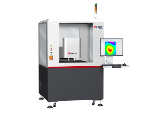
Description
The WD4000 is a specialised system for 3D inspection of unpatterned semiconductor wafers — surface geometry, nanotopography and defect detection at production scale. A niche, high-end tool for semiconductor fabs and materials suppliers. Supplied and supported by SVNM on project basis. (Catalogue pp. 129-134.)
Dimensional Calibration Equipment
Frequently Asked Questions
Yes. SVNM is an authorised distributor of Chotest Technology precision measuring and calibration instruments in India.
SVNM handles model selection, demonstration, installation, operator training and application support for the Unpatterned Wafer 3D Inspection System. Our own NABL-accredited lab can calibrate the equipment after installation.
Get a quote for Unpatterned Wafer 3D Inspection System — Chotest WD4000
Send your drawing or specification and we will reply with a quotation, usually within one working day. Every gauge is supplied with a calibration certificate from our NABL-accredited lab (ISO/IEC 17025, CC-2472).
- Manufacturer and exporter, supplying customers worldwide
- Made to your drawing, standard or sample
- Calibrated in-house before dispatch